Connectors#
This section describes each of the connectors on the board.
Expansion Connectors#
The expansion interface on the board is comprised of two 46 pin connectors. All signals on the expansion headers are _3.3V_ unless otherwise indicated.
NOTE: Do not connect 5V logic level signals to these pins or the board will be damaged.
NOTE: DO NOT APPLY VOLTAGE TO ANY I/O PIN WHEN POWER IS NOT SUPPLIED TO THE BOARD. IT WILL DAMAGE THE PROCESSOR AND VOID THE WARRANTY.
NO PINS ARE TO BE DRIVEN UNTIL AFTER THE SYS_RESET LINE GOES HIGH.
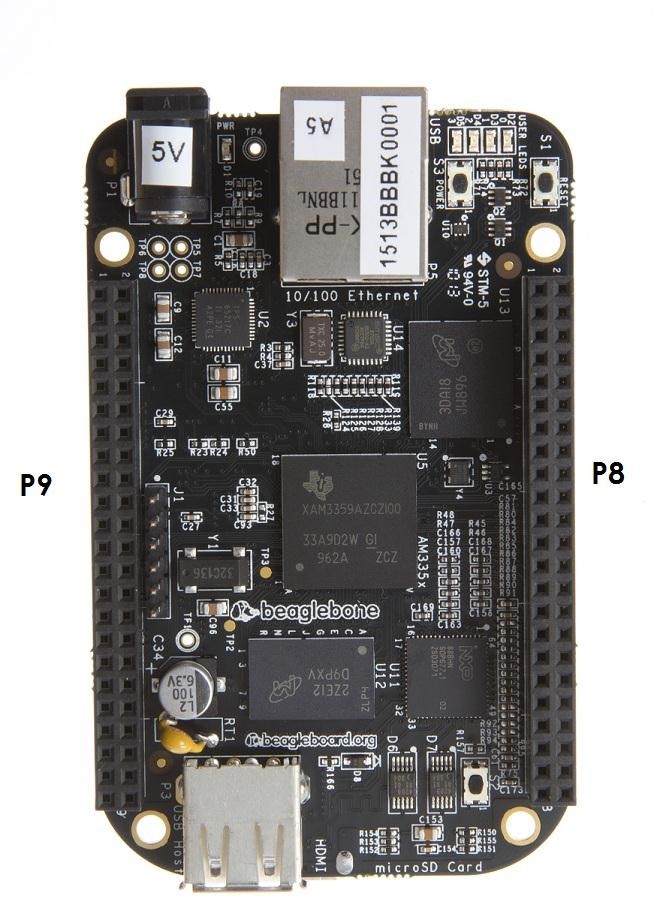
Fig. 217 Expansion Connector Location#
The location and spacing of the expansion headers are the same as on the original BeagleBone.
Connector P8#
table-12 shows the pinout of the P8 expansion header. Other signals can be connected to this connector based on setting the pin mux on the processor, but this is the default settings on power up. The SW is responsible for setting the default function of each pin. There are some signals that have not been listed here. Refer to the processor documentation for more information on these pins and detailed descriptions of all of the pins listed. In some cases there may not be enough signals to complete a group of signals that may be required to implement a total interface.
The PROC column is the pin number on the processor.
The PIN column is the pin number on the expansion header.
The MODE columns are the mode setting for each pin. Setting each mode to align with the mode column will give that function on that pin.
NOTE: DO NOT APPLY VOLTAGE TO ANY I/O PIN WHEN POWER IS NOT SUPPLIED TO THE BOARD. IT WILL DAMAGE THE PROCESSOR AND VOID THE WARRANTY.
NO PINS ARE TO BE DRIVEN UNTIL AFTER THE SYS_RESET LINE GOES HIGH.
PIN |
PROC |
NAME |
MODE0 |
MODE1 |
MODE2 |
MODE3 |
MODE4 |
MODE5 |
MODE6 |
MODE7 |
|---|---|---|---|---|---|---|---|---|---|---|
1,2 |
GND |
|||||||||
3 |
R9 |
GPIO1_6 |
gpmc_ad6 |
mmc1_dat6 |
gpio1[6] |
|||||
4 |
T9 |
GPIO1_7 |
gpmc_ad7 |
mmc1_dat7 |
gpio1[7] |
|||||
5 |
R8 |
GPIO1_2 |
gpmc_ad2 |
mmc1_dat2 |
gpio1[2] |
|||||
6 |
T8 |
GPIO1_3 |
gpmc_ad3 |
mmc1_dat3 |
gpio1[3] |
|||||
7 |
R7 |
TIMER4 |
gpmc_advn_ale |
timer4 |
gpio2[2] |
|||||
8 |
T7 |
TIMER7 |
gpmc_oen_ren |
timer7 |
gpio2[3] |
|||||
9 |
T6 |
TIMER5 |
gpmc_be0n_cle |
timer5 |
gpio2[5] |
|||||
10 |
U6 |
TIMER6 |
gpmc_wen |
timer6 |
gpio2[4] |
|||||
11 |
R12 |
GPIO1_13 |
gpmc_ad13 |
lcd_data18 |
mmc1_dat5 |
mmc2_dat1 |
eQEP2B_in |
pr1_pru0_pru_r30_15 |
gpio1[13] |
|
12 |
T12 |
GPIO1_12 |
gpmc_ad12 |
lcd_data19 |
mmc1_dat4 |
mmc2_dat0 |
eQEP2a_in |
pr1_pru0_pru_r30_14 |
gpio1[12] |
|
13 |
T10 |
EHRPWM2B |
gpmc_ad9 |
lcd_data22 |
mmc1_dat1 |
mmc2_dat5 |
ehrpwm2B |
gpio0[23] |
||
14 |
T11 |
GPIO0_26 |
gpmc_ad10 |
lcd_data21 |
mmc1_dat2 |
mmc2_dat6 |
ehrpwm2_tripzone_in |
gpio0[26] |
||
15 |
U13 |
GPIO1_15 |
gpmc_ad15 |
lcd_data16 |
mmc1_dat7 |
mmc2_dat3 |
eQEP2_strobe |
pr1_pru0_pru_r31_15 |
gpio1[15] |
|
16 |
V13 |
GPIO1_14 |
gpmc_ad14 |
lcd_data17 |
mmc1_dat6 |
mmc2_dat2 |
eQEP2_index |
pr1_pru0_pru_r31_14 |
gpio1[14] |
|
17 |
U12 |
GPIO0_27 |
gpmc_ad11 |
lcd_data20 |
mmc1_dat3 |
mmc2_dat7 |
ehrpwm0_synco |
gpio0[27] |
||
18 |
V12 |
GPIO2_1 |
gpmc_clk_mux0 |
lcd_memory_clk |
gpmc_wait1 |
mmc2_clk |
mcasp0_fsr |
gpio2[1] |
||
19 |
U10 |
EHRPWM2A |
gpmc_ad8 |
lcd_data23 |
mmc1_dat0 |
mmc2_dat4 |
ehrpwm2A |
gpio0[22] |
||
20 |
V9 |
GPIO1_31 |
gpmc_csn2 |
gpmc_be1n |
mmc1_cmd |
pr1_pru1_pru_r30_13 |
pr1_pru1_pru_r31_13 |
gpio1[31] |
||
21 |
U9 |
GPIO1_30 |
gpmc_csn1 |
gpmc_clk |
mmc1_clk |
pr1_pru1_pru_r30_12 |
pr1_pru1_pru_r31_12 |
gpio1[30] |
||
22 |
V8 |
GPIO1_5 |
gpmc_ad5 |
mmc1_dat5 |
gpio1[5] |
|||||
23 |
U8 |
GPIO1_4 |
gpmc_ad4 |
mmc1_dat4 |
gpio1[4] |
|||||
24 |
V7 |
GPIO1_1 |
gpmc_ad1 |
mmc1_dat1 |
gpio1[1] |
|||||
25 |
U7 |
GPIO1_0 |
gpmc_ad0 |
mmc1_dat0 |
gpio1[0] |
|||||
26 |
V6 |
GPIO1_29 |
gpmc_csn0 |
gpio1[29] |
||||||
27 |
U5 |
GPIO2_22 |
lcd_vsync |
gpmc_a8 |
pr1_pru1_pru_r30_8 |
pr1_pru1_pru_r31_8 |
gpio2[22] |
|||
28 |
V5 |
GPIO2_24 |
lcd_pclk |
gpmc_a10 |
pr1_pru1_pru_r30_10 |
pr1_pru1_pru_r31_10 |
gpio2[24] |
|||
29 |
R5 |
GPIO2_23 |
lcd_hsync |
gpmc_a9 |
pr1_pru1_pru_r30_9 |
pr1_pru1_pru_r31_9 |
gpio2[23] |
|||
30 |
R6 |
GPIO2_25 |
lcd_ac_bias_en |
gpmc_a11 |
gpio2[25] |
|||||
31 |
V4 |
UART5_CTSN |
lcd_data14 |
gpmc_a18 |
eQEP1_index |
mcasp0_axr1 |
uart5_rxd |
uart5_ctsn |
gpio0[10] |
|
32 |
T5 |
UART5_RTSN |
lcd_data15 |
gpmc_a19 |
eQEP1_strobe |
mcasp0_ahclkx |
mcasp0_axr3 |
uart5_rtsn |
gpio0[11] |
|
33 |
V3 |
UART4_RTSN |
lcd_data13 |
gpmc_a17 |
eQEP1B_in |
mcasp0_fsr |
mcasp0_axr3 |
uart4_rtsn |
gpio0[9] |
|
34 |
U4 |
UART3_RTSN |
lcd_data11 |
gpmc_a15 |
ehrpwm1B |
mcasp0_ahclkr |
mcasp0_axr2 |
uart3_rtsn |
gpio2[17] |
|
35 |
V2 |
UART4_CTSN |
lcd_data12 |
gpmc_a16 |
eQEP1A_in |
mcasp0_aclkr |
mcasp0_axr2 |
uart4_ctsn |
gpio0[8] |
|
36 |
U3 |
UART3_CTSN |
lcd_data10 |
gpmc_a14 |
ehrpwm1A |
mcasp0_axr0 |
uart3_ctsn |
gpio2[16] |
||
37 |
U1 |
UART5_TXD |
lcd_data8 |
gpmc_a12 |
ehrpwm1_tripzone_in |
mcasp0_aclkx |
uart5_txd |
uart2_ctsn |
gpio2[14] |
|
38 |
U2 |
UART5_RXD |
lcd_data9 |
gpmc_a13 |
ehrpwm0_synco |
mcasp0_fsx |
uart5_rxd |
uart2_rtsn |
gpio2[15] |
|
39 |
T3 |
GPIO2_12 |
lcd_data6 |
gpmc_a6 |
eQEP2_index |
pr1_pru1_pru_r30_6 |
pr1_pru1_pru_r31_6 |
gpio2[12] |
||
40 |
T4 |
GPIO2_13 |
lcd_data7 |
gpmc_a7 |
eQEP2_strobe |
pr1_edio_data_out7 |
pr1_pru1_pru_r30_7 |
pr1_pru1_pru_r31_7 |
gpio2[13] |
|
41 |
T1 |
GPIO2_10 |
lcd_data4 |
gpmc_a4 |
eQEP2A_in |
pr1_pru1_pru_r30_4 |
pr1_pru1_pru_r31_4 |
gpio2[10] |
||
42 |
T2 |
GPIO2_11 |
lcd_data5 |
gpmc_a5 |
eQEP2B_in |
pr1_pru1_pru_r30_5 |
pr1_pru1_pru_r31_5 |
gpio2[11] |
||
43 |
R3 |
GPIO2_8 |
lcd_data2 |
gpmc_a2 |
ehrpwm2_tripzone_in |
pr1_pru1_pru_r30_2 |
pr1_pru1_pru_r31_2 |
gpio2[8] |
||
44 |
R4 |
GPIO2_9 |
lcd_data3 |
gpmc_a3 |
ehrpwm0_synco |
pr1_pru1_pru_r30_3 |
pr1_pru1_pru_r31_3 |
gpio2[9] |
||
45 |
R1 |
GPIO2_6 |
lcd_data0 |
gpmc_a0 |
ehrpwm2A |
pr1_pru1_pru_r30_0 |
pr1_pru1_pru_r31_0 |
gpio2[6] |
||
46 |
R2 |
GPIO2_7 |
lcd_data1 |
gpmc_a1 |
ehrpwm2B |
pr1_pru1_pru_r30_1 |
pr1_pru1_pru_r31_1 |
gpio2[7] |
Connector P9#
Table-13 lists the signals on connector P9. Other signals can be connected to this connector based on setting the pin mux on the processor, but this is the default settings on power up.
There are some signals that have not been listed here. Refer to the processor documentation for more information on these pins and detailed descriptions of all of the pins listed. In some cases there may not be enough signals to complete a group of signals that may be required to implement a total interface.
The PROC column is the pin number on the processor.
The PIN column is the pin number on the expansion header.
The MODE columns are the mode setting for each pin. Setting each mode to align with the mode column will give that function on that pin.
NOTES:
In the table are the following notations:
PWR_BUT is a 5V level as pulled up internally by the TPS65217C. It is activated by pulling the signal to GND.
NOTE: DO NOT APPLY VOLTAGE TO ANY I/O PIN WHEN POWER IS NOT SUPPLIED TO THE BOARD. IT WILL DAMAGE THE PROCESSOR AND VOID THE WARRANTY.
NO PINS ARE TO BE DRIVEN UNTIL AFTER THE SYS_RESET LINE GOES HIGH.
Both of these signals connect to pin 41 of P11. Resistors are installed that allow for the GPIO3_20 connection to be removed by removing R221. The intent is to allow the SW to use either of these signals, one or the other, on pin 41. SW should set the unused pin in input mode when using the other pin. This allowed us to get an extra signal out to the expansion header.
Both of these signals connect to pin 42 of P11. Resistors are installed that allow for the GPIO3_18 connection to be removed by removing R202. The intent is to allow the SW to use either of these signals, on pin 42. SW should set the unused pin in input mode when using the other pin. This allowed us to get an extra signal out to the expansion header.
PIN |
PROC |
NAME |
MODE0 |
MODE1 |
MODE2 |
MODE3 |
MODE4 |
MODE5 |
MODE6 |
MODE7 |
|---|---|---|---|---|---|---|---|---|---|---|
1,2 |
GND |
|||||||||
3,4 |
DC_3.3V |
|||||||||
5,6 |
VDD_5V |
|||||||||
7,8 |
SYS_5V |
|||||||||
9 |
PWR_BUT |
|||||||||
10 |
A10 |
SYS_RESETn |
||||||||
11 |
T17 |
UART4_RXD |
gpmc_wait0 |
mii2_crs |
gpmc_csn4 |
rmii2_crs_dv |
mmc1_sdcd |
uart4_rxd_mux2 |
gpio0[30] |
|
12 |
U18 |
GPIO1_28 |
gpmc_be1n |
mii2_col |
gpmc_csn6 |
mmc2_dat3 |
gpmc_dir |
mcasp0_aclkr_mux3 |
gpio1[28] |
|
13 |
U17 |
UART4_TXD |
gpmc_wpn |
mii_rxerr |
gpmc_csn5 |
rmii2_rxerr |
mmc2_sdcd |
uart4_txd_mux2 |
gpio0[31] |
|
14 |
U14 |
EHRPWM1A |
gpmc_a2 |
mii2_txd3 |
rgmii2_td3 |
mmc2_dat1 |
gpmc_a18 |
ehrpwm1A_mux1 |
gpio1[18] |
|
15 |
R13 |
GPIO1_16 |
gpmc_a0 |
gmii2_txen |
rmii2_tctl |
mii2_txen |
gpmc_a16 |
ehrpwm1_tripzone_input |
gpio1[16] |
|
16 |
T14 |
EHRPWM1B |
gpmc_a3 |
mii2_txd2 |
rgmii2_td2 |
mmc2_dat2 |
gpmc_a19 |
ehrpwm1B_mux1 |
gpio1[19] |
|
17 |
A16 |
I2C1_SCL |
spi0_cs0 |
mmc2_sdwp |
I2C1_SCL |
ehrpwm0_synci |
pr1_uart0_txd |
gpio0[5] |
||
18 |
B16 |
I2C1_SDA |
spi0_d1 |
mmc1_sdwp |
I2C1_SDA |
ehrpwm0_tripzone |
pr1_uart0_rxd |
gpio0[4] |
||
19 |
D17 |
I2C2_SCL |
uart1_rtsn |
timer5 |
dcan0_rx |
I2C2_SCL |
spi1_cs1 |
pr1_uart0_rts_n |
gpio0[13] |
|
20 |
D18 |
I2C2_SDA |
uart1_ctsn |
timer6 |
dcan0_tx |
I2C2_SDA |
spi1_cs0 |
pr1_uart0_cts_n |
gpio0[12] |
|
21 |
B17 |
UART2_TXD |
spi0_d0 |
uart2_txd |
I2C2_SCL |
ehrpwm0B |
pr1_uart0_rts_n |
EMU3_mux1 |
gpio0[3] |
|
22 |
A17 |
UART2_RXD |
spi0_sclk |
uart2_rxd |
I2C2_SDA |
ehrpwm0A |
pr1_uart0_cts_n |
EMU2_mux1 |
gpio0[2] |
|
23 |
V14 |
GPIO1_17 |
gpmc_a1 |
gmii2_rxdv |
rgmii2_rxdv |
mmc2_dat0 |
gpmc_a17 |
ehrpwm0_synco |
gpio1[17] |
|
24 |
D15 |
UART1_TXD |
uart1_txd |
mmc2_sdwp |
dcan1_rx |
I2C1_SCL |
pr1_uart0_txd |
pr1_pru0_pru_r31_16 |
gpio0[15] |
|
25 |
A14 |
GPIO3_21 |
mcasp0_ahclkx |
eQEP0_strobe |
mcasp0_axr3 |
mcasp1_axr1 |
EMU4_mux2 |
pr1_pru0_pru_r30_7 |
pr1_pru0_pru_r31_7 |
gpio3[21] |
26 |
D16 |
UART1_RXD |
uart1_rxd |
mmc1_sdwp |
dcan1_tx |
I2C1_SDA |
pr1_uart0_rxd |
pr1_pru1_pru_r31_16 |
gpio0[14] |
|
27 |
C13 |
GPIO3_19 |
mcasp0_fsr |
eQEP0B_in |
mcasp0_axr3 |
mcasp1_fsx |
EMU2_mux2 |
pr1_pru0_pru_r30_5 |
pr1_pru0_pru_r31_5 |
gpio3[19] |
28 |
C12 |
SPI1_CS0 |
mcasp0_ahclkr |
ehrpwm0_synci |
mcasp0_axr2 |
spi1_cs0 |
eCAP2_in_PWM2_out |
pr1_pru0_pru_r30_3 |
pr1_pru0_pru_r31_3 |
gpio3[17] |
29 |
B13 |
SPI1_D0 |
mcasp0_fsx |
ehrpwm0B |
spi1_d0 |
mmc1_sdcd_mux1 |
pr1_pru0_pru_r30_1 |
pr1_pru0_pru_r31_1 |
gpio3[15] |
|
30 |
D12 |
SPI1_D1 |
mcasp0_axr0 |
ehrpwm0_tripzone |
spi1_d1 |
mmc2_sdcd_mux1 |
pr1_pru0_pru_r30_2 |
pr1_pru0_pru_r31_2 |
gpio3[16] |
|
31 |
A13 |
SPI1_SCLK |
mcasp0_aclkx |
ehrpwm0A |
spi1_sclk |
mmc0_sdcd_mux1 |
pr1_pru0_pru_r30_0 |
pr1_pru0_pru_r31_0 |
gpio3[14] |
|
32 |
VADC |
|||||||||
33 |
C8 |
AIN4 |
||||||||
34 |
AGND |
|||||||||
35 |
A8 |
AIN6 |
||||||||
36 |
B8 |
AIN5 |
||||||||
37 |
B7 |
AIN2 |
||||||||
38 |
A7 |
AIN3 |
||||||||
39 |
B6 |
AIN0 |
||||||||
40 |
C7 |
AIN1 |
||||||||
41 |
D14 |
CLKOUT2 |
xdma_event_intr1 |
tclkin |
clkout2 |
timer7_mux1 |
pr1_pru0_pru_r31_16 |
EMU3_mux0 |
gpio0[20] |
|
D13 |
GPIO3_20 |
mcasp0_axr1 |
eQEP0_index |
mcasp1_axr0 |
emu3 |
pr1_pru0_pru_r30_6 |
pr1_pru0_pru_r31_6 |
gpio3[20] |
||
42 |
C18 |
GPIO0_7 |
eCAP0_in_PWM0_out |
uart3_txd |
spi1_cs1 |
pr1_ecap0_ecap_capin_apwm_o |
spi1_sclk |
mmc0_sdwp |
xdma_event_intr2 |
gpio0[7] |
B12 |
GPIO3_18 |
mcasp0_aclkr |
eQEP0A_in |
mcasp0_axr2 |
mcasp1_aclkx |
pr1_pru0_pru_r30_4 |
pr1_pru0_pru_r31_4 |
gpio3[18] |
||
43-46 |
GND |
Power Jack#
The DC power jack is located next to the RJ45 Ethernet connector as shown in <<figure-51>>. This uses the same power connector as is used on the original BeagleBone. The connector has a 2.1mm diameter center post (5VDC) and a 5.5mm diameter outer dimension on the barrel (GND).
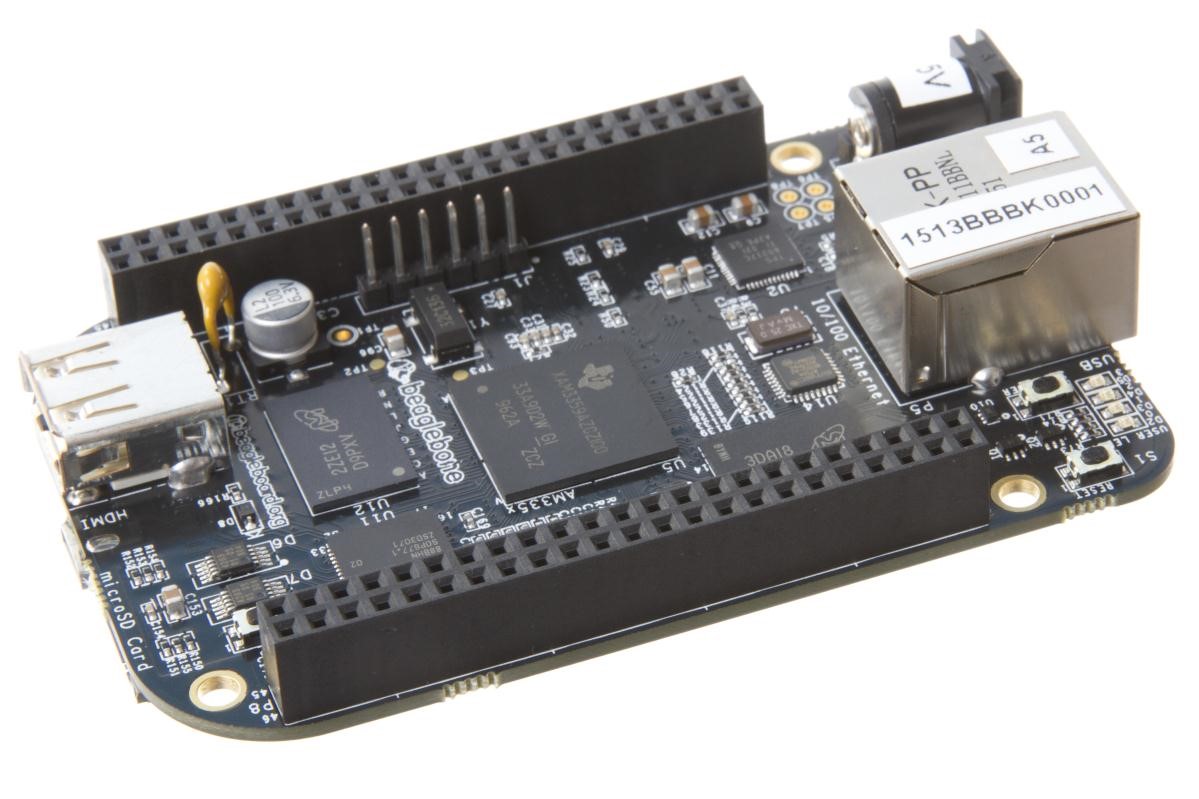
Fig. 218 5VDC Power Jack#
The board requires a regulated 5VDC +/-.25V supply at 1A. A higher current rating may be needed if capes are plugged into the expansion headers. Using a higher current power supply will not damage the board.
USB Client#
The USB Client connector is accessible on the bottom side of the board under the row of four LEDs as shown in <<figure-52>>. It uses a 5 pin miniUSB cable, the same as is used on the original BeagleBone. The cable is provided with the board. The cable can also be used to power the board.
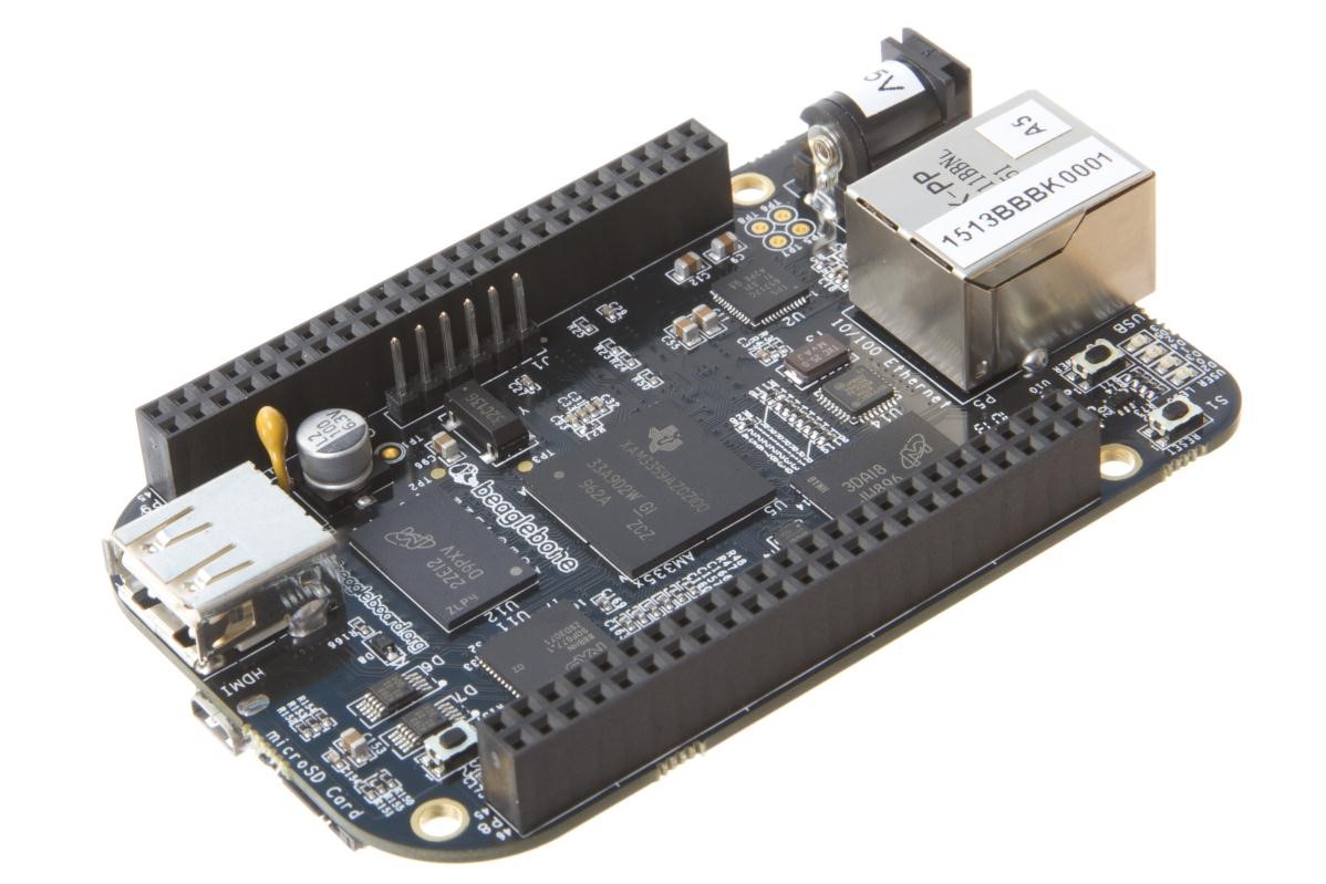
Fig. 219 USB Client#
This port is a USB Client only interface and is intended for connection to a PC.
USB Host#
There is a single USB Host connector on the board and is shown in Figure 53 below.

Fig. 220 USB Host Connector#
The port is USB 2.0 HS compatible and can supply up to 500mA of current. If more current or ports is needed, then a HUB can be used.
Serial Header#
Each board has a debug serial interface that can be accessed by using a special serial cable that is plugged into the serial header as shown in Figure 54 below.

Fig. 221 Serial Debug Header#
Todo
Make all figure references actual references
Two signals are provided, TX and RX on this connector. The levels on these signals are 3.3V. In order to access these signals, a FTDI USB to Serial cable is recommended as shown in Figure 55 below.
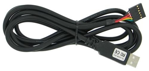
Fig. 222 PRU-ICSS Block Diagram#
The cable can be purchased from several different places and must be the 3.3V version TTL-232R-3V3. Information on the cable itself can be found direct from FTDI at: pdf
Todo
move accessory links to a single common document for all boards.
Pin 1 of the cable is the black wire. That must align with the pin 1 on the board which is designated by the white dot next to the connector on the board.
Refer to the support WIKI http://elinux.org/BeagleBoneBlack for more sources of this cable and other options that will work.
Todo
We should include all support information in docs.beagleboard.org now and leave eLinux to others, freeing it as much as possible
Table is the pinout of the connector as reflected in the schematic. It is the same as the FTDI cable which can be found at https://ftdichip.com/wp-content/uploads/2020/07/DS_USB_RS232_CABLES.pdf with the exception that only three pins are used on the board. The pin numbers are defined in Table 14. The signals are from the perspective of the board.
PIN NUMBER |
SIGNAL |
|---|---|
1 |
Ground |
4 |
Receive |
5 |
Transmit |
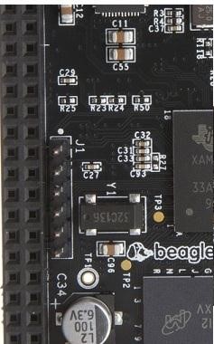
Fig. 223 Serial Header#
HDMI#
Access to the HDMI interface is through the HDMI connector that is located on the bottom side of the board as shown in Figure 57 below.

Fig. 224 HDMI Connector#
The connector is microHDMI connector. This was done due to the space limitations we had in finding a place to fit the connector. It requires a microHDMI to HDMI cable as shown in Figure 58 below. The cable can be purchased from several different sources.
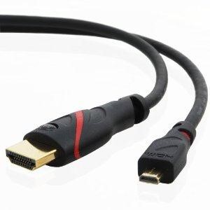
Fig. 225 HDMI Cable#
microSD#
A microSD connector is located on the back or bottom side of the board as shown in Figure 59 below. The microSD card is not supplied with the board.

Fig. 226 microSD Connector#
When plugging in the SD card, the writing on the card should be up. Align the card with the connector and push to insert. Then release. There should be a click and the card will start to eject slightly, but it then should latch into the connector. To eject the card, push the SD card in and then remove your finger. The SD card will be ejected from the connector.
Do not pull the SD card out or you could damage the connector.
Ethernet#
The board comes with a single 10/100 Ethernet interface located next to the power jack as shown in Figure below.

Fig. 227 Ethernet Connector#
The PHY supports AutoMDX which means either a straight or a swap cable can be used.
JTAG Connector#
A place for an optional 20 pin CTI JTAG header is provided on the board to facilitate the SW development and debugging of the board by using various JTAG emulators. This header is not supplied standard on the board. To use this, a connector will need to be soldered onto the board.
If you need the JTAG connector you can solder it on yourself. No other components are needed. The connector is made by Samtec and the part number is FTR-110-03-G-D-06. You can purchase it from http://www.digikey.com/

